
Sensor Integration and Signal processing Part I
SNR
Definition of SNR
What is a good sensor?
Definition: SNR
SNR (signal-to-noise ratio) : defined as the ratio of signal power to noise power, typically expressed in decibels (dB)
Low Noise!
- Electronic noise is a random fluctuation in an electrical signal, a characteristic of all electronic circuits.
- Johnson–Nyquist noise (thermal noise, Johnson noise, or Nyquist noise) is the electronic noise generated by the thermal agitation of the charge carriers (usually the electrons) inside an electrical conductor at equilibrium.
- Shot noise, flicker noise, burst/popcorn noise, Avalanche noise…
Wheatstone bridge*
How to improve the SNR:
- Voltage divider:
- Wheatstone bridge
is resistive sensor is matched to nominal value of - If
and (nominal), varies as changes
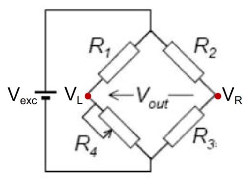
For Wheatstone bridge: Assume:
where
Then:
Common temperature drift can be compensated!
If the bridge circuit is balanced:
Signal process
Fourier Transform
Analog low-pass filter
Impedance: Ohm’s law:
not
- Resistor:
- Capacitor:
; low impedance for high frequency - Inductor:
; high impedance for high frequency
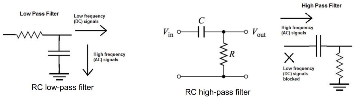
Definition: Low-pass filters
In an ideal low-pass filter's, the frequency between pass and stop bands is called the cut-off frequency (
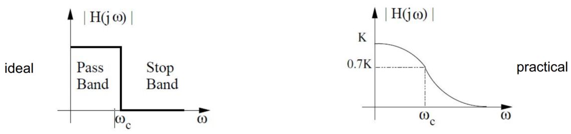
In practical filters, pass and stop bands are not clearly defined,
The cut-off frequency is, therefore, defined as the frequency at which
RL filter
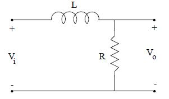
To find the cut-off frequency, we note
RC filter
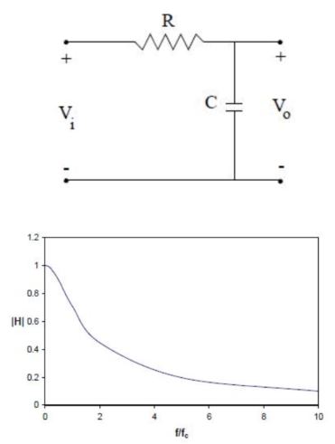
To find cut-off frequency (Similar to RL filter)
RL and RC filters above are part of the family of first-order filters (they include only one capacitor or inductor). In general, the voltage transfer function of a first-order low-pass filter is in the form:
High-Pass Filter
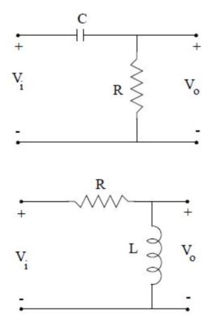
- RC filter
- RL filter
DAQ
Definition: DAQ
Data acquisition (DAQ): is the process of sampling signals that measure real world physical conditions and converting the resulting samples into digital numeric values that can be manipulated by a computer.
- physical system
- Transducer sensor
- Signal conditioning
- Analog-Digital converter
- Computer
Example: A temperature control system
- Thermal sensor (input)
- Microcontroller (processor)
- Electrical heater (output)
ADC
Definition: ADC
Analog-to-Digital converter (ADC, A/D, or A-to-D) is a system that converts an analog signal, such as a sound picked up by a microphone or light entering a digital camera, into a digital signal.
An ADC may also provide an isolated measurement such as an electronic device that converts an input analog voltage or current to a digital number representing the magnitude of the voltage or current.
Example: LM35
Sensor output is a voltage (analog signal)
LM35 is a low cost temperature sensor
- Basic Centigrade (2°C to 150°C)
- typical accuracy of 0.25°C at room temperature and 0.75°C for full range.
- output voltage has a scale factor of
per degree
- 10-bit ADC: divide
by converted to
When using
Sensor resolution
Definition: resolution
The resolution of a sensor is the smallest change it can detect in the quantity that it is measuring.
The resolution of a sensor with a digital output is usually the resolution of the digital output.
The resolution is related to the precision with which the measurement is made, but they are not the same thing. A sensor's accuracy may be considerably worse than its resolution.
For example:
The more bits an ADC has, the higher resolution we can achieve
Sampling
Definition
- In signal processing, sampling is the reduction of a continuous-time signal to a discrete-time signal. A common example is the conversion of a sound wave (a continuous signal) to a sequence of samples (a discrete-time signal).
- A sample is a value or set of values at a point in time and/or space. A sampler is a subsystem or operation that extracts samples from a continuous signal. A theoretical ideal sampler produces samples equivalent to the instantaneous value of the continuous signal at the desired points.
- For functions that vary with time, let
be a continuous function (or "signal") to be sampled, and let sampling be performed by measuring the value of the continuous function every seconds, which is called the sampling interval or the sampling period. Then the sampled function is given by the sequence:
- The sampling frequency or sampling rate,
, is the average number of samples obtained in one second (samples per second), thus .
Aliasing~
- Aliasing: Output signal due to sampling frequency of the sensor?
- An aliased signal provides a poor representation of the analog signal. Aliasing causes a false lower frequency component to appear in the sampled data of a signal.
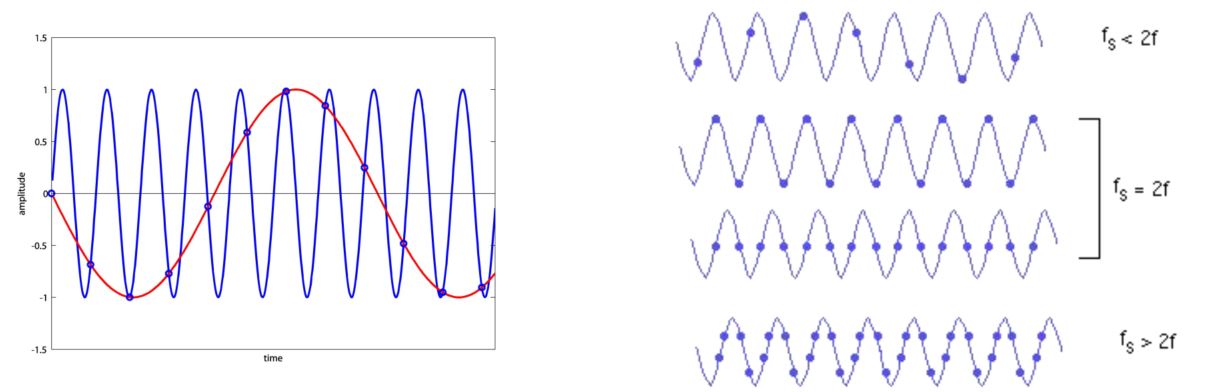
When
The Poisson summation formula indicates that the samples are sufficient to create a periodic summation of
which is a periodic function and its equivalent representation as a Fourier series. This function is also known as the discrete-time Fourier transform (DTFT) of the sample sequence.
Any frequency component above
Two anti-aliasing solutions:
- Increase the sample rate to cover all frequencies, i.e.,
- Use low pass filter: When the sample-rate is pre-determined by other considerations (such as an industry standard),
is usually filtered to reduce its high frequencies to acceptable levels before it is sampled. The type of filter required is a lowpass filter, and in this application it is called an anti-aliasing filter.
Sampling Theorem
- The Nyquist–Shannon sampling theorem serves as a fundamental bridge between continuous-time signals and discrete-time signals.
- It establishes a sufficient condition for a sample rate that permits a discrete sequence of samples to capture all the information from a continuous-time signal of finite bandwidth.
- Increasing the sampling frequency increases the number of data points acquired in a given time period.
- A fast sampling frequency provides a better representation of the original signal than a slower sampling frequency.
- For a given sampling frequency, the maximum frequency you can accurately represent without aliasing is the Nyquist frequency. The Nyquist frequency equals one-half the sampling frequency
where is the sampling frequency.
DAC
Definition: DAC
Digital to Analog Converter (DAC) is a device that transforms digital data into an analog signal.
D/A Converter Architectures:
- Weighted resistors method (the inverting summing amplifier)
- simple design and low cost
- As the number of bits is increasing, the range of the resistor values becomes large and accordingly, the accuracy becomes poor.
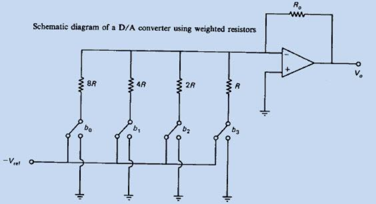
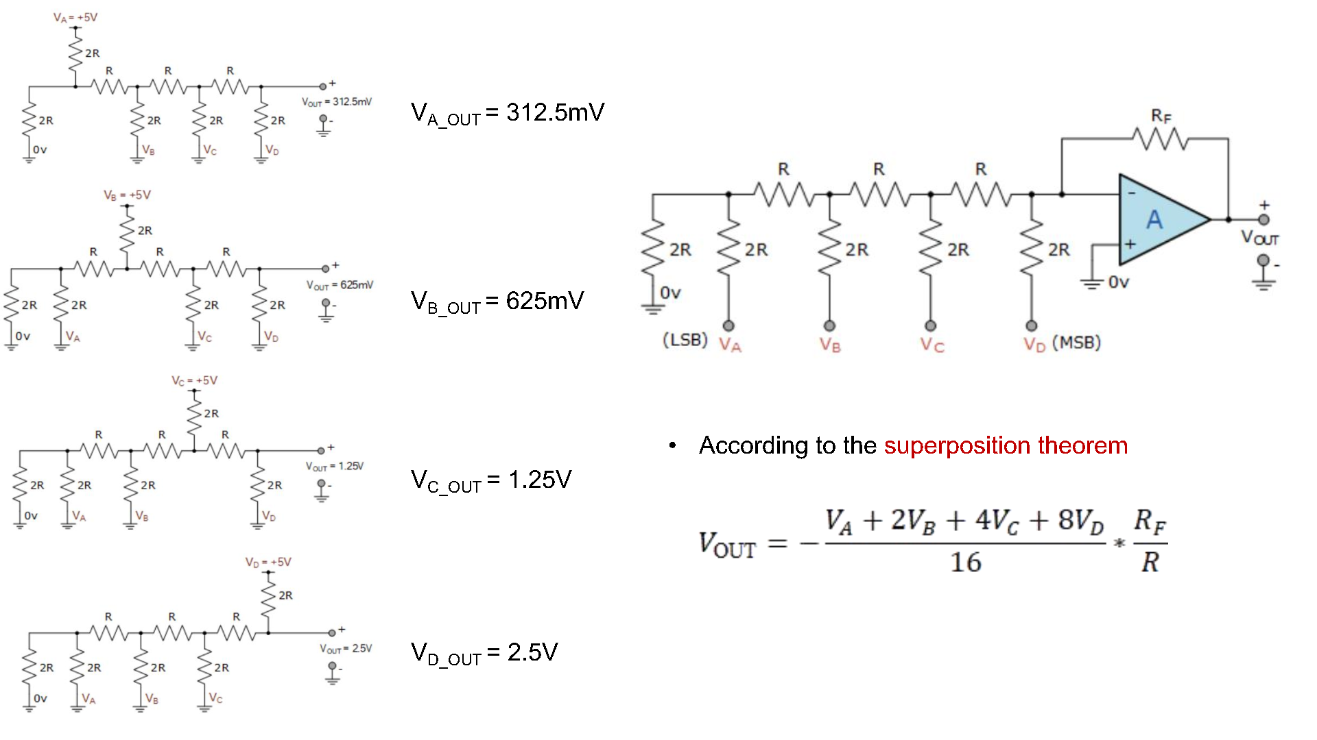
This is a 4-bit DAC example:
- R-2R ladder method
- Only two value of resistors used
- The actual value is less important
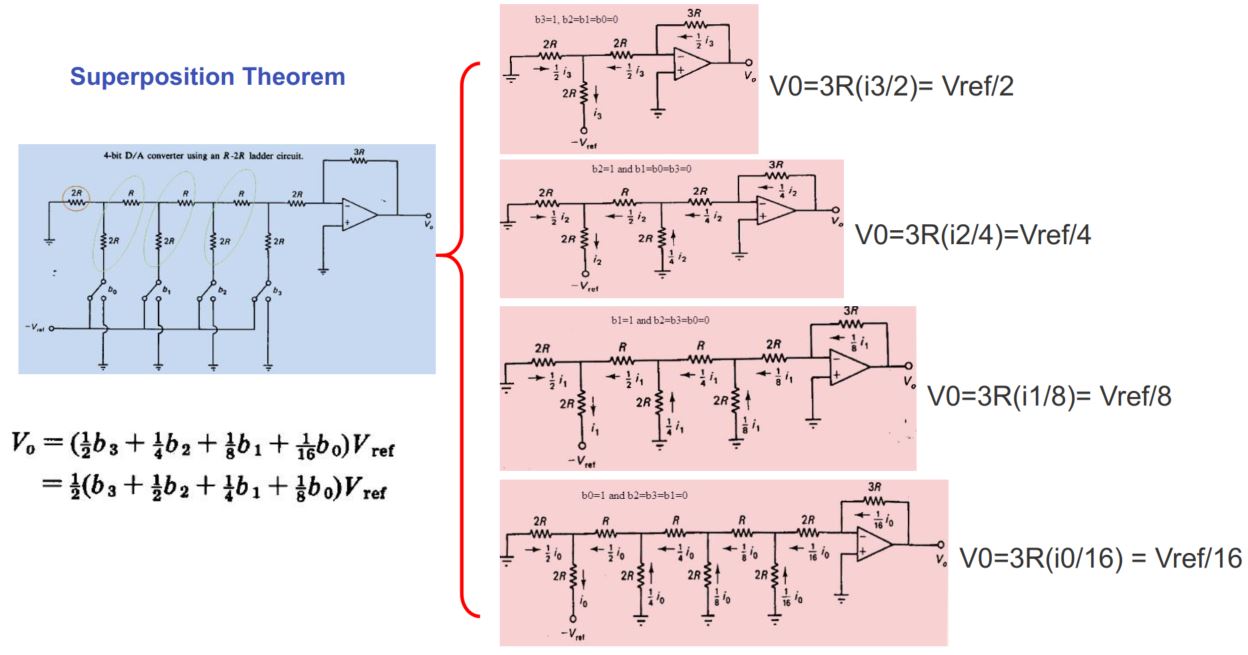
Both methods are called the binary-weighted DAC
R-2R ladder method
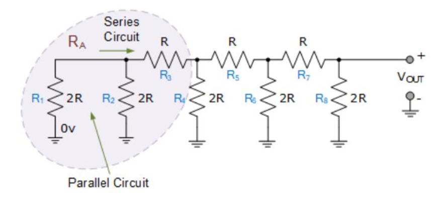
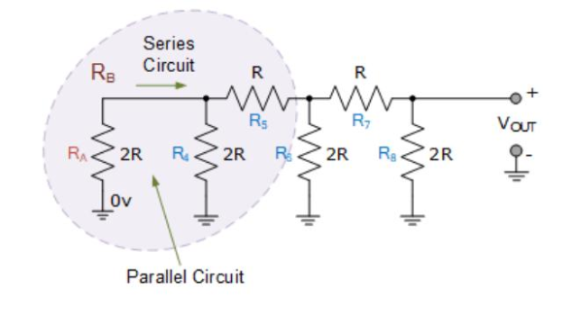
Similarly:
And finally,
- The op-amp input is at virtual ground
- Current into the op-amp stage:
- Output voltage:
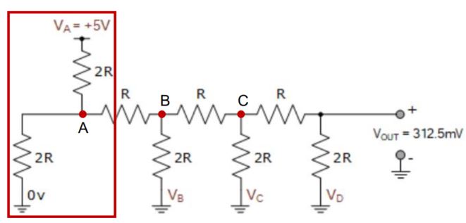
The two
- Thevenin equivalent voltage (
): These two resistors form a voltage divider.
- Thevenin equivalent resistance (
): Set the voltage source to zero (short circuit to ground), the equivalent resistance seen from node A is two resistors in parallel.
Similarly:
Applications & limitations
Applications
- Audio amplifier
- Video encoder
- Display electronics
- Motion control
Limitations of binary-weighted DAC
- Use multi-channel GPIO
- It requires very accurate resistors, as the DAC would require that the error in each resistor be less than the smallest resistor value.
- If n = 10, we need a resistor
PWM as DAC
PWM - pulse width modulation
- control the speed of DC motor
- control the brightness of LED
The duty cycle
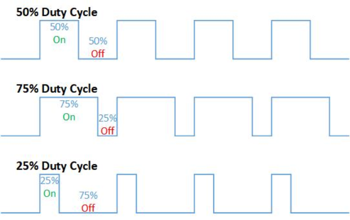
Why PWM can work as DAC
- Desired DAC voltage =
is the amplitude of the PWM (i.e., for LPC1743 ARM processor)
Fourier analysis of PWM as DAC voltage output: Assume we have a PWM:
. frequency is ; the rise and fall times are both . Use a low-pass filter:
- We want a stable
; don’t want the troublesome highfrequency spike (i.e., , …) - Use a low-pass filter in a PWM DAC: the filter retains the DC component while suppressing everything else.
- We want a stable
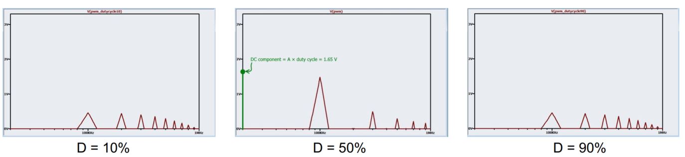
When
Set
- When
:
- When
:
where
- When
:
Trade-off:
- A lower cutoff frequency means less ripple and longer settling time; a higher cutoff frequency means more ripple and shorter settling time.
- Higher-order filters improve performance, but they also increase cost and complexity. Instead of spending time and money implementing a fancy filter for a mediocre PWM DAC, we should just use an external DAC!
An Easy Way to Improve PWM DAC: just increase the frequency of the PWM signal!
- E.g., change
to - Same RC filter with
, the settling time is only about