Silicon Bulk Micromachining for MEMS
Basic Integrated Fabrication Process
Introduction: Silicon as the Premier Material for Microsystems
While the global semiconductor industry was built upon the electronic properties of silicon, the field of MEMS requires a fundamental shift in perspective. As engineers, we must move beyond viewing Single-Crystal Silicon (SCS) merely as a carrier for transistors. In the realm of micromachining, silicon is leveraged as a high-performance structural material—a medium for the fabrication of microscopic beams, membranes, and springs.
The transition from Integrated Circuit (IC) design to MEMS fabrication necessitates this "mechanical rethink": where an IC designer sees a semiconductor for switching, a MEMS engineer sees a mechanical substrate with a yield strength superior to steel and a mass density comparable to aluminum. Bulk Micromachining is the primary technique used to realize these 3D geometries by etching directly into the substrate bulk.
Silicon as a Substrate: Material Properties and Advantages
Engineers leverage SCS for 6 definitive reasons that make it the ideal substrate for microsystems:
- Monolithic Integration: Silicon is mechanically stable and permits the direct integration of electronics. Sensing elements, such as p-type or n-type piezoresistors, can be diffused directly into the structural Si substrate for seamless signal transduction.
- Structural Excellence: It is an almost ideal structural material. It maintains a linear relationship between applied load and induced deformation, crucial for precision sensors.
- High-Temperature Dimensional Stability: With a melting point of 1400°C (nearly twice that of aluminum), silicon remains dimensionally stable during high-temperature deposition and annealing cycles.
- Low Thermal Drift: The thermal expansion coefficient (
) is roughly 8 times smaller than steel and 10 times smaller than aluminum, significantly reducing thermal noise in sensitive measurements. - Negligible Mechanical Hysteresis: Because SCS is a single crystal, it exhibits virtually no mechanical hysteresis. This property is the cornerstone of reliability for actuators and sensors requiring high repeatability.
- Established Fabrication Ecosystem: Silicon benefits from decades of documented fabrication processes, including precise thin-film coatings and established lithography standards.
Silicon is stiff => Thinning is required for appreciable strain
Engineering Insight on Stiffness: While silicon is exceptionally stiff (
Why / Why not silicon?
- Semiconductor: Active Devices + Sensors (Photo-Magneto-Strain Sensing)
- Insulator:
, Glass - Thin Film Conductor: Aluminum, Gold, Silicides
- Photolithography: Planar control (+ & -)
Micromachining of Silicon?
- Additive Processes: Chemical and Physical Deposition (Thin Layers only) (Single/Poly)
- Removal Processes: Chemical and Physical Etching (Wet/Dry/Plasma/Inert/Reactive) (Bulk/Film) (Anisotropic/Isotropic)
Micromatching of Silicon
- Bulk (substrate)
- Surface (films)
The Manufacturing of Single-Crystal Silicon
The fabrication pipeline initiates with the production of a defect-free, high-purity silicon boule.
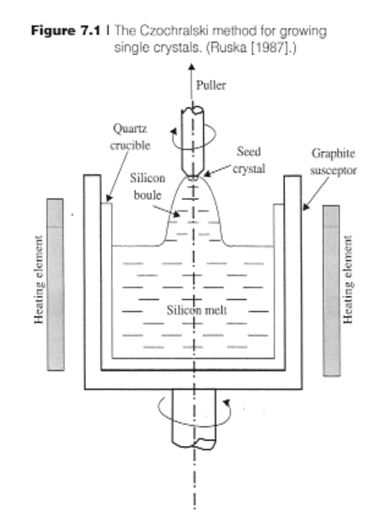
The Czochralski process involves melting high-purity silicon in a quartz crucible within a graphite susceptor. A seed crystal is introduced to the melt and slowly withdrawn while rotating, allowing the silicon to crystallize into a continuous, single-crystal lattice (the boule).
Wafer Orientation and Identification: Before slicing, "flats" are ground into the boule to provide visual identification of the crystal orientation and doping type
Structure of Single Crystal Silicon
- Primary Flat: Ground perpendicular to the crystal axis to indicate orientation (typically {110} or {100}).
- Secondary Flat: Positioned relative to the primary flat. In n-type wafers, the secondary flat is ground at a 45° angle from the primary flat; in p-type wafers, the secondary flat placement varies (e.g., 90°) or may be absent to distinguish the electrical characteristics.
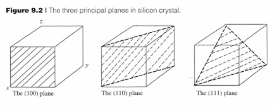
Crystallography and Miller Indices
Silicon crystallizes in a diamond lattice structure, which can be visualized as two interpenetrating Face-Centered Cubic (FCC) sub-lattices. This structure dictates the material's inherent anisotropy—the variation of properties based on direction.
Atom Density Synthesis: To calculate the number of atoms per cubic centimeter (
Miller Indices (hkm): The coordinate system (hkm) defines the crystal planes based on their intercepts with the
Etching for bulk micromatching
- Normal Planes (001), (010), (100): These define the faces of the cubic unit cell.
- Diagonal Planes (110): Intersect two axes, cutting the cell at 45°.
- Inclined Planes (111): Intersect all three axes, forming the most densely packed planes in the silicon lattice.
SCS has anisotropic properties: Electrical, Thermal, Mechanical, Chemical
Applied Anisotropy: Because of this lattice structure, the mechanical stiffness (
| Orientation | Young's Modulus (E, GPa) | Shear Modulus (G, GPa) |
|---|---|---|
| <100> | 129.5 | 79.0 |
| <110> | 168.0 | 61.7 |
| <111> | 186.5 | 57.5 |
The Basic Integrated Fabrication Cycle
The realization of 3D micro-geometry is a circular, iterative process. Most MEMS devices require dozens of these cycles to build complexity.
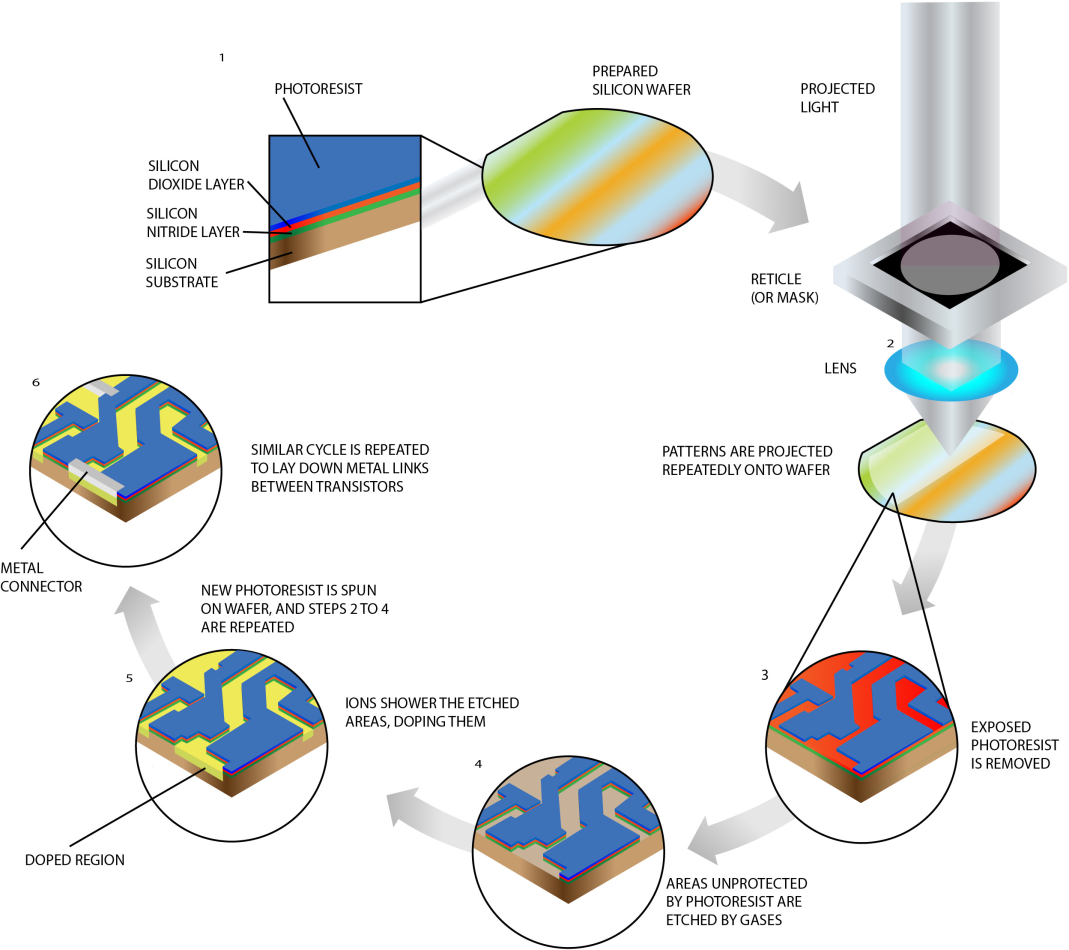
- Substrate Preparation: Layers of insulators (
) are deposited on the substrate. - Photolithography: Photoresist is spun on, and a reticle (mask) pattern is projected via UV light.
- Development: Exposed photoresist is removed, leaving a protective pattern.
- Etching (Removal): Unprotected areas of the thin films or the bulk substrate are removed via gas-phase or liquid etchants.
- Doping: The wafer is showered with ions to alter the electrical conductivity in specific regions (creating junctions or piezoresistors).
- Metallization & Repeat: Metal connectors (
) are deposited, and the cycle repeats to add subsequent structural layers.
Core Concept: Fabrication is the balance of Additive Processes (CVD/PVD deposition of thin films) and Removal Processes (wet/dry etching of the bulk or films).
- Bulk Micromachining: Principles of Etching
The defining characteristic of Bulk Micromachining is the removal of material from the substrate itself to create structures like trenches, cavities, and suspended membranes.
Linking Crystallography to Geometry: The orientation of the silicon crystal (Miller Indices) directly determines the final etched shape when using Anisotropic etchants (e.g., KOH). In anisotropic wet etching, the etch rate is highly direction-dependent; the {111} planes etch much slower than the {100} planes.
- Result: Etching a (100) wafer with an anisotropic etchant creates a characteristic V-groove where the sidewalls are the {111} planes, sloping at an angle of 54.7°.
- Isotropic Etching: Conversely, isotropic etchants (usually acid-based) remove material at the same rate in all directions, resulting in rounded, bowl-like cavities.
Using these principles, we can engineer complex mechanical parts:
- Part (a/b): V-grooves and trenches defined by crystal planes.
- Part (c/d): Suspended proof masses and springs for accelerometers, achieved by "undercutting" the bulk material.
Examples of Bulk Micromachined Structures: Micro Thermal-Chemical Power