Surface Micromachining
Understanding the Micro-Scale
In the field of Micro-Electro-Mechanical Systems (MEMS), precision is dictated by our mastery of the microscopic world. To engineer effectively at this level, we must first establish a rigorous definition of the scales involved.
Definition and Scales:
The "micro" scale is anchored by the micrometer (
- meso scale:
or . - Micrometer (
): or . - Nanometer (
): or . - Angstrom (Å):
or .
Size Comparison Analysis:
To contextualize these dimensions, consider how common entities compare to the standard MEMS device range of 1 to 1,000
- Human hair:
- Bacteria:
- Tobacco smoke:
- Integrated Circuit (IC) elements:
- Viruses:
- MEMS/micromachines:
The "Why it Matters" Summary Understanding these scale differences is critical because physical constraints change as we move from the meso (millimeter) scale to the micro and nano scales. At these dimensions, a single speck of dust is a mountain. Manufacturing precision requires specialized techniques to manage the physical properties of thin films and the extreme environmental factors that can lead to device failure.
The Controlled Environment: Clean Room Standards
Micro-fabrication cannot occur in a standard laboratory. Microscopic debris, such as skin cells or lint, is often larger than the mechanical elements of a MEMS device, leading to catastrophic structural interference.
Environmental Control Fabrication requires a "Clean Room" where air quality, humidity, and temperature are strictly regulated. Standards typically require a constant humidity of 45% and a temperature of 70°F.
Class Definitions Clean rooms are categorized by "Class," defined by the maximum number of particles larger than
Clean Room Class Max Particles (
- Class 100: < 100 particles (size
) - Modern VLSI: Class 10 to Class 1
Practical Application:
These environmental controls ensure that microscopic particles do not contaminate thin films during deposition or interfere with the pattern transfer during lithography, preventing structural defects in the final micromachines.
The Core Methodology: Add, Lithograph, Subtract
- The foundation of both IC and MEMS technology
- Allows parallel "manufacturing" of millions of parts simultaneous and consistently.
Process Overview The cycle consists of three repeating stages:
Add Thin Film
- Add: Add by deposition, oxidation, electroplating etc.
- Subtract: Etch by ions, gas, or chemicals, etc.
Photolithography
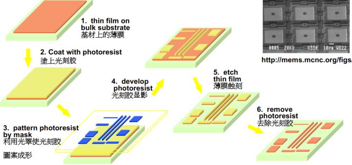
Deep-Dive ultra violet(UV) Lithography is the process used to transfer a pattern from a mask to the substrate.
The process follows six technical steps:
- Bulk Substrate: Begin with the base material (typically a Silicon wafer).
- Coating: Apply a thin film of Photoresist (PR), a photosensitive polymer.
- Masking: Cover the PR with a pre-patterned mask.
- Developing: Expose to UV light and place in a developing solution to reveal the pattern.
- Etching: Subtract the thin film in areas not protected by the PR.
- Stripping: Remove the remaining PR to conclude the subtraction phase.
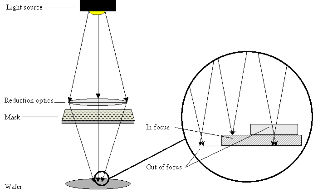
Technical Limits The resolution (minimum width
- Typical light source: UV light; wave length
to ( to )
As technology has progressed, the limit of photolithography size reduction has moved from
PR thickness
where
Thin Film Addition: Growth and Deposition
Adding materials to a substrate is achieved through two distinct philosophies: growth and deposition.
Growth vs. Deposition
Growth: Requires a "seed" material from the substrate (基材). For example, Silicon Dioxide (
) can be grown from a Silicon (Si) substrate. Thermal Oxidation:
is grown by heating Si to in either pure oxygen or water. - Dry Oxidation:
- Wet Oxidation:
- Deal-Grove Model:
- For short durations, specifically when
, the oxide thickness is calculated as .
- For short durations, specifically when
- Dry Oxidation:
Deposition: Material is placed on top of a substrate. This does not require a chemical relationship with the base material (e.g., depositing Gold on Silicon).
- Thermal Evaporation (Physical Vapor Deposition)
- E-Beam Evaporation (Physical Vapor Deposition)
- Sputtering (Physical Vapor Deposition)
- Chemical Vapor "Deposition"
Thermal Evaporation
Evaporation of thin films take place in a vacuum environment.
Note:
- Physical Vapor Deposition (PVD) PVD occurs in a vacuum to prevent oxidation and ensure uniform coverage.
- A vacuum system can be classified based on its chamber pressure
- High vacuum:
to - Very high vacuum:
to - Ultrahigh vacuum: below
- High vacuum:
- This is a unit of pressure, NOT a unit of distance.
The mean-free-path of gas particles is about
where
The rate at which atoms pass into vacuum from a heated source is given by the Hertz-Knudsen equation:
where
Thus, the evaporated flux from a small source of area
where
The thickness growth rate of the film is given by:
Where
Summary of Thermal Evaporation
- Source materials: aluminum (
), copper ( ), nickel ( ), chromium ( ), titanium ( ), gold ( ), , …etc. - Chamber condition: high vacuum to control composition of the deposited materials (
to ) - Prevents oxidation (low moisture in a vacuum chamber)
- Allows uniform coverage
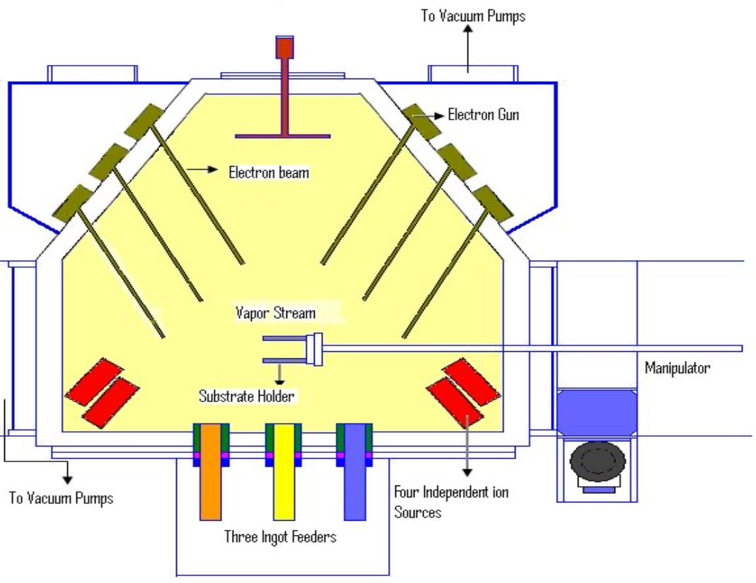
E-Beam Evaporation
- Basically same as Thermal Evaporation, except that an electron-beam is used to melt source materials (instead of a resistive coil (电阻线圈) that is used in thermal evaporation systems)
- Source materials: same as thermal evaporation, i.e.,
, …etc. - The source material is not in direct contact with a filament as in the case of thermal evaporation. This non-contact evaporation will allow cleaner materials to be deposited.
Melting Temperatures of various commonly used MEMS materials
| Target | Melting Pt (°C) | Temp at 10^{-2} Torr (°C) |
|---|---|---|
| Aluminum (Al) | 659 | 1220 |
| Chromium (Cr) | ~1900 | 1400 |
| Copper (Cu) | 1084 | 1260 |
| Gold (Au) | 1063 | 1400 |
| Nickel (Ni) | 1450 | 1530 |
| Platinum (Pt) | 1770 | 2100 |
| Silicon (Si) | 1410 | 1350 |
| Titanium (Ti) | 1700 | 1750 |
| Tungsten (W) | 3380 | 3230 |
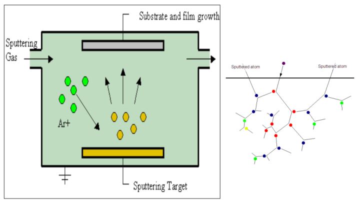
Sputtering
A momentum transfer process * no chemical or composition change of material.
- Source material: almost anything.
- Atoms for molecules at source (target) surface are "knocked off" by energized gas ions (e.g.,
) and deposit on the wafer. - More expensive than evaporation
Sputtering "Yields":
- However, Sigmund’s linear cascade theory correlates well with experimental values in the near-linear energy range and has become widely used:
where
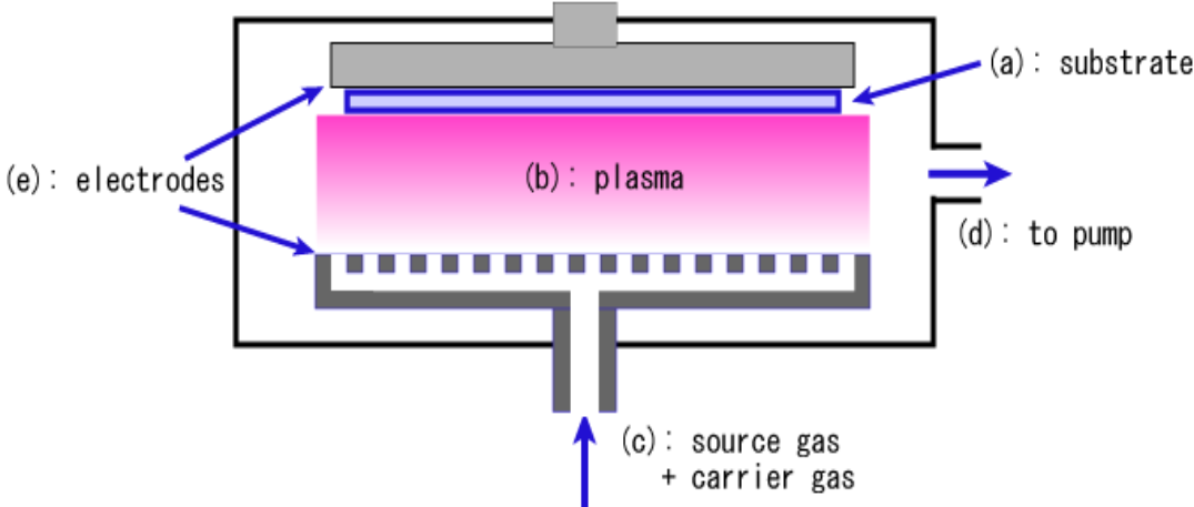
Chemical Vapor Deposition (CVD) CVD involves chemical interactions between gas precursors and the substrate.
Ion energy and sputtering yield for various MEMS related materials
| Target | Ion Energy (eV) | Yield (atoms/ion) |
|---|---|---|
| Au | 600 | 2.8 |
| Cr | 600 | 1.3 |
| Pt | 600 | 1.6 |
| Al | 500 | 1.0 |
| Si | 500 | 0.5 |
| Cu | 500 | 2.4 |
Chemical Vapor "Deposition"
Chemical interaction between vapor and substrate
CVD
Example:
- Silicon Nitride:
( + gas by products) - Silicon Nitride:
( + gas by products) - Polysilicon:
- Silicon Dioxide:
Various types:
- LPCVD (Low Pressure):
- Operates at ~0.5 Torr;
- Long gas mean-free-path
- Excellent step coverage.
- PECVD (Plasma Enhanced)
- Same as LPCVD, but grows discharge plasma during deposition
- Lower deposition temperature than LPCVD
- Film quality worst than LPCVC
Electroplating 电镀
- A classical method to “grow” metals
- Requires a seed layer
- The term electroplating means the coating of an object with a thin layer of metal by use of electricity. The metals most often used are gold, silver, chromium, copper, nickel, tin and zinc, but many others are used also. The object to be plated is usually a different metal, but can be the same metal or a non-metal.
- Useful for "LIGA" micromachining process.
Spin-on coating
Thickness:
- Materials such as photoresist and polyimide (widely used as a passivation layer for IC chips and as a structural material for MEMS devices)
- Polyimid (survives up to
) used to build MEMS devices has the following disadvantage: - May be unstable over time mechanically
- Attracts moisture
- Generally, materials which are in viscous-fluidic form at room temperature can be spin-coated, i.e., liquid polymers.
Thin Film Subtraction: Etching Fundamentals
Etching Metrics
- A process is selective if it etches the desired material at a high rate and all other exposed surfaces at lower rates.
- Selectivity (
): The ratio of the etch rate of material A to material B. High selectivity is required to ensure the etchant removes the target film without destroying the mask or substrate. - Isotropy/Anisotropy: Isotropic etches are non-directional (rounded sidewalls), while anisotropic etches are directional (vertical sidewalls).
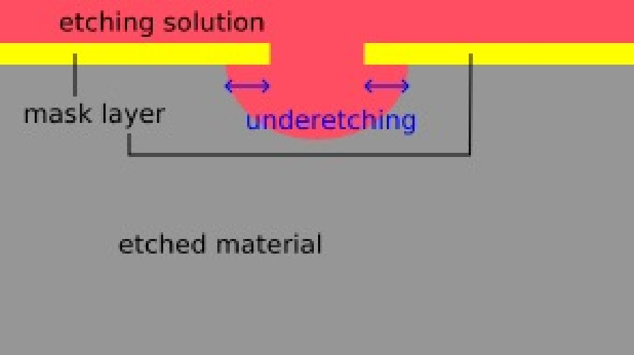
Wet Etching
Completely based on chemical reactions
- Polysilicon Etch
- Etched with Nitric and Hydrofluoric (HF) acid at room temperature.
- Mask: Nitride or photoresist (not for too long)
- Etchrate at ~400 Å/min for
doped polysilicon - ~1500 Å/min for undoped polysilicon
- Nitride Etch
- Nitride is very hard to etch, so it's a good mask for many processes
- Use hot Phosphoric Acid (
) - Etchrate: ~80 Å/min at 180°C. The etch rate is strongly dependent on film composition, i.e., the stoichiometry (
and values for ). - Mask:
~1 Å/min
- Oxide Etch (
) - Use HF at room temperature.
- Mask: photoresist, polysilicon, nitride
- Etchrate: dry oxide < wet oxide < CVD oxide
- With 49% HF ==> 23,000 Å /min for wet oxide; 36,000 Å /min for phosphosilicate glass(PSG)
- With 5:1 of
: HF mixture ==> 1,000 Å /min for wet oxide; 7,000 Å /min for PSG
The advantage of wet etching is that it gives good selectivity but its resolution limit is only
Dry Etching and Plasma
Plasma (等离子体) is a highly ionized gas with local electric charges that produce physical and chemical etching effects.
Doping Effects: In plasma etching, heavily n-type doped Polysilicon etches much faster than p-type or undoped versions.
Gas Profiles: Fluorine-based gases (
) generally etch isotropically, while Chlorine-based gases ( ) provide anisotropic profiles. Polysilicon
- Poly-Si can be etched by
and based gases such as , and . based gases generally etch isotropically while based gases can yield anisotropic profiles. - For heavily n-type doped poly-Si, the etch rate is >> undoped poly-Si
- For p-type doped poly-Si, the etch rate is indistinguishable from undoped poly-Si.
- Poly-Si can be etched by
Thermal and LPCVD Oxide
can be etched by and . , and etch ansiotropically under most operating conditions. and can etch ansiotropically only under specific operating conditions. - Etch rate: PSG > LPCVD
> thermal . (Rate of psg can be (thermal- ))
Sputtering yields are generally determined experimentally. However, Sigmund’s linear cascade theory correlates well with experimental values in the near-linear energy range and has become widely used.
Example: Micro Hinge
The "Pister Hinge" demonstrates how surface micromachining creates moving mechanical parts through the use of sacrificial layers.
Fabrication Sequence
- Grow a sacrificial SiO_2 layer on a Silicon substrate.
- Apply Photoresist (PR).
- Expose and develop the PR to define a "bar" pattern.
- Etch the SiO_2 to create the sacrificial support.
- Deposit a structural Polysilicon layer over the SiO_2 bar.
- Apply a second PR layer.
- Expose and develop to define the hinge beam.
- Etch the Polysilicon structural layer.
- Strip the PR.
- Final Release: Remove the SiO_2 sacrificial layer with HF, leaving a free-standing, movable Polysilicon beam.
Summary
- Surface Micromachining
- Thin film addition
- UV Photolithography
- Thin film subtraction
Q: What are the common Si-based materials used to build MEMS devices?
Common silicon-based materials used in the construction of MEMS devices include:
- Single Crystalline Silicon (Si): This is typically used as the bulk substrate or base material for the devices.
- Polysilicon (Poly-Si): This is a primary structural material used to build components like beams and hinges. It is often deposited using Chemical Vapor Deposition (CVD).
- Silicon Dioxide (
): This material is pervasive in MEMS for electrical insulation, as a masking material, or as a sacrificial layer that is later removed to release moving parts. It can be "grown" through thermal oxidation or deposited via CVD. - Silicon Nitride (
or ): It is frequently used as a masking material because it is very hard to etch, but it can also serve as a structural layer. - Amorphous Silicon: This form of silicon is specifically mentioned as a material used in Plasma-Enhanced Chemical Vapor Deposition (PECVD) processes.
- Phosphosilicate Glass (PSG): Often categorized with oxides, PSG is used in thin-film addition and is sometimes referred to as Low Temperature Oxide (LTO).
These materials are typically applied to a substrate through a process of adding thin films, patterning them via photolithography, and then subtracting (etching) them to create complex microscopic structures.
Q: What are the key techniques to add thin films?
Key techniques for adding thin films in micro-fabrication and MEMS technology include growth, deposition, electroplating, and spin-on coating.
Thin Film Growth (Thermal Oxidation) Growth requires a proper "seed" material to initiate the process. The most common example is thermal oxidation, where silicon (
) is heated to temperatures between 900 and 1200 °C in either pure oxygen (dry oxidation) or water vapor (wet oxidation) to grow silicon dioxide ( ). This material is widely used for electrical insulation or as a masking layer. Deposition Techniques Deposition is categorized into two main physical and chemical processes:
- Physical Vapor Deposition (PVD):
- Thermal Evaporation: Uses a resistive coil to heat and evaporate source materials (like
, or ) in a high vacuum environment. - E-Beam Evaporation: Similar to thermal evaporation, but utilizes an electron beam to melt the source material. Because the material is not in direct contact with a filament, it allows for cleaner deposited films.
- Sputtering: A momentum transfer process where energized gas ions (typically
) "knock off" atoms from a target material, which then deposit onto the wafer. This process is more expensive than evaporation but can be used for almost any material.
- Thermal Evaporation: Uses a resistive coil to heat and evaporate source materials (like
- Chemical Vapor Deposition (CVD): This involves a chemical interaction between a vapor and the substrate.
- LPCVD (Low Pressure CVD): Performed at low pressure (~0.5 torr) to ensure a long gas mean-free-path and excellent step coverage.
- PECVD (Plasma Enhanced CVD): Uses discharge plasma to allow for lower deposition temperatures than LPCVD, though the film quality is generally lower.
- Physical Vapor Deposition (PVD):
Electroplating This is a classical method used to grow metals (such as gold, silver, copper, and nickel) by using electricity. It requires a seed layer and is particularly useful for the "LIGA" micromachining process.
Spin-on Coating This technique is used for materials that are in viscous-fluidic form at room temperature, such as liquid polymers. A uniform layer is achieved by spinning the wafer at high speeds.
- Common Materials: Photoresist (PR) and polyimide.
- Thickness Control: The thickness (
) is controlled by the angular velocity ( ), viscosity, and solid content of the solution.
Q: What are the key techniques to subtract thin films?
The key techniques to subtract thin films, also known as etching, are categorized into two primary methods: wet etching and dry etching.
Wet Etching This technique is completely based on chemical reactions between an etching solution and the thin film material.
- Mechanism: The wafer is immersed in a liquid chemicals that attack the targeted material but ideally not the masking layer (like photoresist).
- Advantages: It typically offers good selectivity, meaning it can etch one material much faster than others.
- Disadvantages: It has a resolution limit of approximately 3 µm and often suffers from under-cutting (under-etching), where the chemicals etch horizontally beneath the mask.
- Common Examples:
- Polysilicon: Etched using Nitric acid (
) and Hydrofluoric acid (HF). - Silicon Dioxide (
): Etched using HF or Buffered Oxide Etch (BOE). - Silicon Nitride (
): Etched using hot phosphoric acid ( ) at 180°C.
- Polysilicon: Etched using Nitric acid (
Dry Etching Dry etching uses gases, ions, or plasma to remove material rather than liquid chemicals.
- Plasma Etching: This involves using a highly ionized gas, or plasma, to produce chemical or physical effects on the target layer. It can be isotropic (producing round sidewalls) or anisotropic (producing vertical sidewalls) depending on the gases used.
- Fluorine-based gases (like
or ) generally etch isotropically. - Chlorine-based gases (like
) can yield anisotropic profiles.
- Fluorine-based gases (like
- Sputtering: This is a physical momentum transfer process where energized ions "knock off" atoms from the target surface.
- Reactive Ion Etching (RIE): A common form of dry etching mentioned for materials like Parylene using
plasma to achieve specific etch rates.
- Plasma Etching: This involves using a highly ionized gas, or plasma, to produce chemical or physical effects on the target layer. It can be isotropic (producing round sidewalls) or anisotropic (producing vertical sidewalls) depending on the gases used.
Key Concepts in Subtraction
- Selectivity: A process is considered selective if it etches the desired material at a high rate while leaving other exposed surfaces (like the substrate or mask) relatively untouched.
- Isotropy vs. Anisotropy: Isotropic etches progress in all directions equally (round sidewalls), while anisotropic etches are directional (vertical sidewalls), which is often preferred for high-precision micro-structures.